XCEED MP – Multi-Purpose 3D AOI
Multi-purpose 3D AOI system delivering component, solder, and conformal coating inspection in one machine—eliminating the need for separate inspection systems.
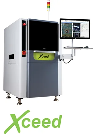
Product Overview
The PARMI Xceed MP is an advanced multi-purpose 3D Automated Optical Inspection system designed to consolidate critical inspection tasks into a single platform. Using a precision Laser Line Scan Method, the Xceed MP performs component inspection, solder joint analysis, and conformal coating verification—all within one machine and without adding cycle time. This consolidation allows manufacturers to streamline their SMT production lines while maintaining comprehensive quality control.
At the core of the Xceed MP is its software-configurable architecture, which supports SPI (Solder Paste Inspection), AOI (Automated Optical Inspection), and CCI (Conformal Coating Inspection) modes according to user needs. The system measures height, area, and volume with 3D precision, detecting defects such as positional misalignment, solder bridging, shape anomalies, foreign material contamination, and PCB warpage. Automatic compensation for PCB shrinkage and expansion ensures measurement accuracy across varying board conditions.
The Xceed MP is engineered for integration into modern smart factory environments, offering feedback and feedforward connectivity for real-time process optimization. By providing actionable inspection data upstream and downstream in the production line, manufacturers can identify root causes of defects, reduce scrap, and continuously improve yield. Distributed and supported by TIIHTRONICS across Mexico and Texas.
Key Features
- Laser Line Scan Method for high-precision 3D measurement and defect detection
- Multi-purpose inspection covering components, solder, and conformal coating in a single pass
- Software configurable to SPI, AOI, or CCI modes based on user needs
- 3D measurement of height, area, and volume for comprehensive defect analysis
- Component positional misalignment detection for accurate placement verification
- Solder bridge and shape anomaly detection for joint-level defect catching
- Foreign material and contamination identification on PCB surfaces
- PCB warpage detection and measurement for board-level quality assessment
- Automatic PCB shrinkage and expansion compensation ensuring measurement accuracy
- Feedback and feedforward connectivity enabling closed-loop process optimization
- Conformal coating coverage verification with 3D height-based analysis
- Backed by TIIHTRONICS local service, training & support in Mexico and Texas